As the semiconductor industry continues to push the boundaries of Moore’s Law, new technologies are emerging to overcome the physical and electrical limitations of traditional FinFET architectures. One such groundbreaking development is the Gate-All-Around (GAA) transistor architecture, which promises to deliver significant performance and power efficiency improvements as the industry scales down to the nanometer era.
Let’s learn what GAA is all about, what it does to improve upon FinFET, and how long it should be before adoption ramps up.
The GAA Concept

Gate-All-Around technology is a novel approach to transistor design that encases the semiconductor channel with gates on all sides. Unlike the conventional planar transistors where the gate is placed on top of the channel, or the FinFET design where the gate wraps around three sides of a fin-shaped channel, GAA transistors as the name implies surrounds the entire channel.
This allows the gate to better control the flow of current through the transistor meaning that more current can flow through with less leakage, and a lower gate voltage is needed to operate the transistor. In addition, the geometry makes it possible for engineers to pack more transistors in a chip, advancing Moore’s Law even further.
Advantages of GAA
Compared to FinFET, GAA has several advantages:
- Reduced Power Consumption: With lower leakage currents and improved channel control, GAA transistors offer significant power efficiency, crucial for battery-operated and low-power devices.
- Enhanced Electrostatic Control: The all-around gate structure provides superior electrostatic control over the channel, reducing leakage currents and improving overall performance.
- Scalability: GAA transistors are better suited for scaling to smaller technology nodes, facilitating the development of more compact and efficient devices.
- Improved Performance: The enhanced control over the channel leads to higher drive currents and faster switching speeds, contributing to better overall device performance.
Electrical Performance
Gate-All-Around transistors offer superior drive current capabilities and lower off-current levels compared to FinFETs, leading to faster and more energy-efficient switching. The improved control over the channel also reduces the short-channel effects and enhances the overall performance of integrated circuits.
Manufacturing Challenges
While GAA offers compelling benefits, transitioning from FinFET to GAA technology presents significant manufacturing challenges. The complexity of creating a structure where the gate material wraps around the channel requires advanced etching and deposition techniques. Additionally, the industry needs to develop new materials and processes to manage the increased strain on the channel, which affects electron mobility and device performance.
Industry Adoption
GAA should be in use by basically all chips from 2025 onwards. All major players in the chip manufacturing industry have announced not only having it figured out but roadmaps as to when it will be implemented and their future iterations.
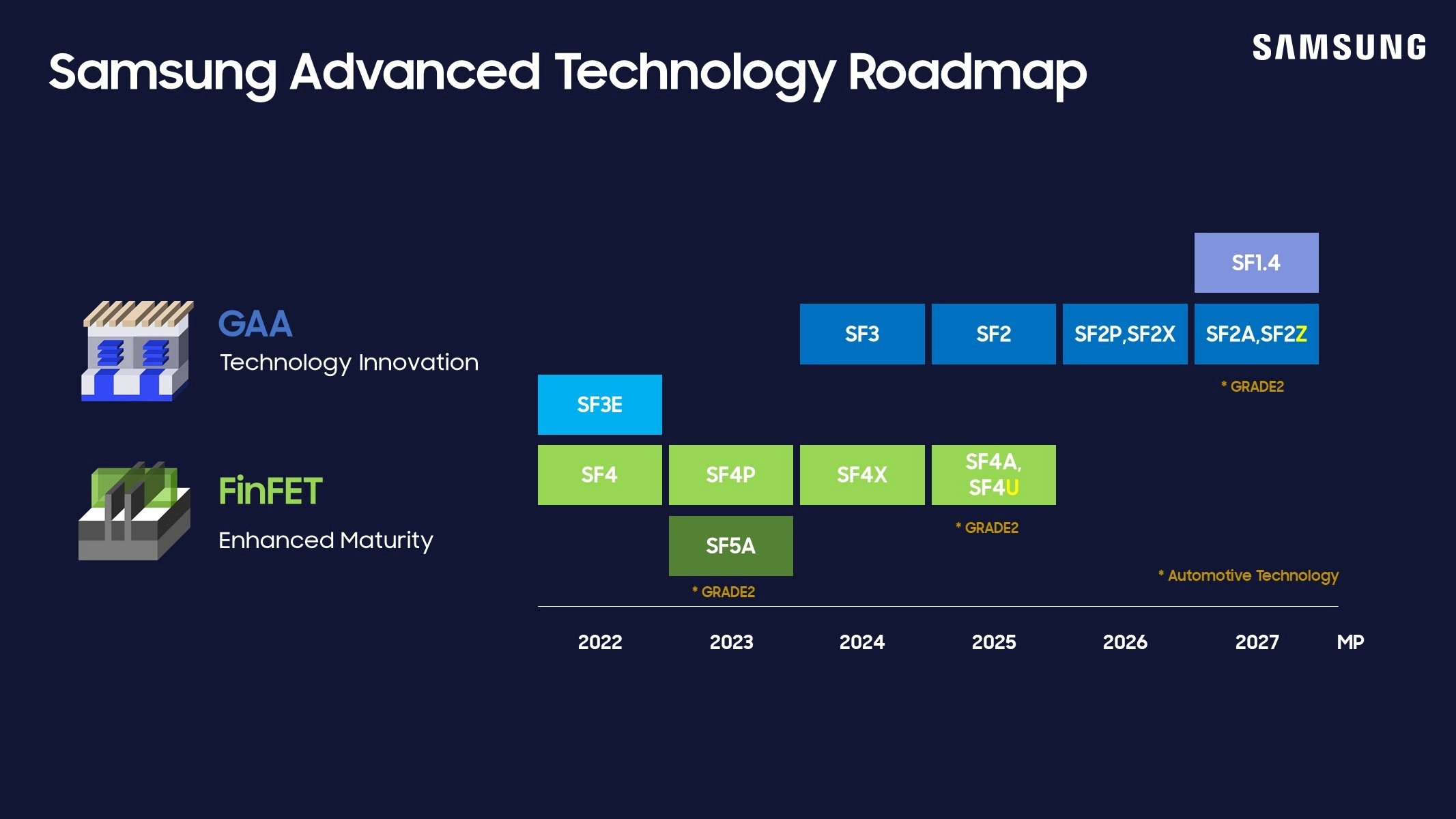
Samsung announced their first experimental node made public back in 2022 with SF3E node(“E” here standing for early), with more polished versions expected for this year(SF3, non E) and new iterations each year after.

Intel, despite current setbacks and clear lack of technology, goes one step further. They intend to implement Gate-All-Around(18A) alongside back power delivery, both technologies that promise to improve efficiency and performance.
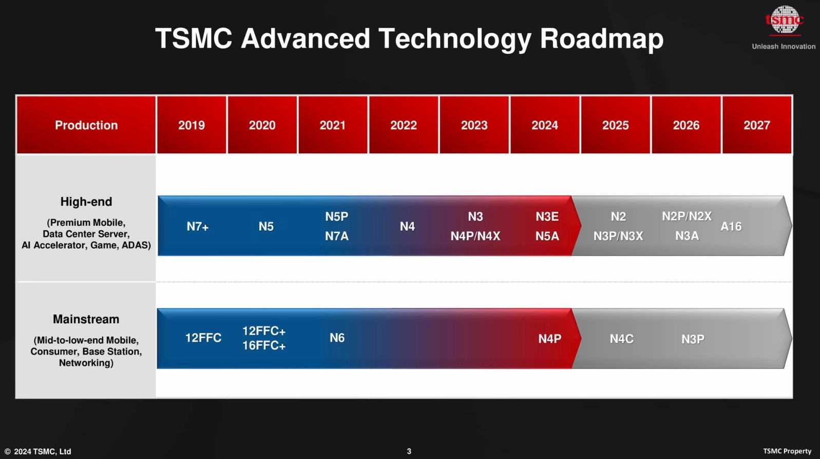
Finally, TSMC is a bit more conservative. They promise GAA next year with the new N2 process family, and back power delivery much later, in 2027, with the A16.
Like my content? Support me with a tip!